1. Project Overview
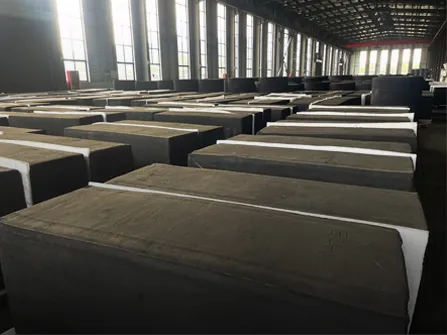
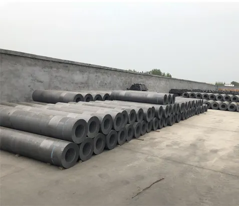
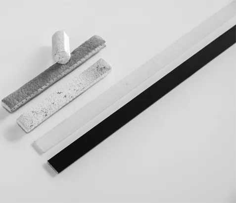
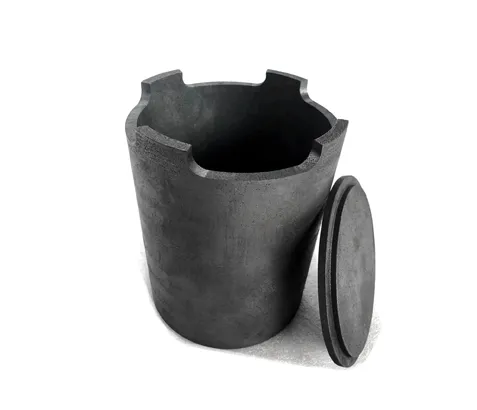
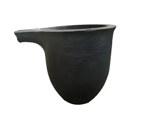
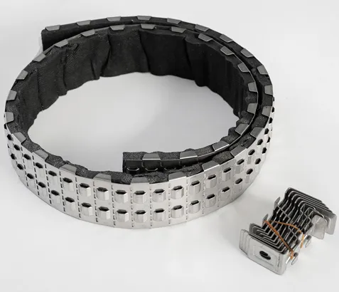
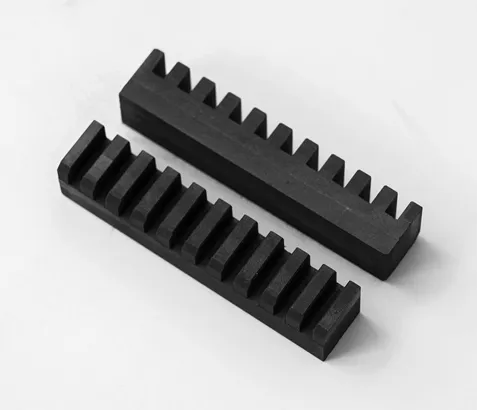
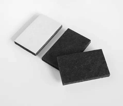
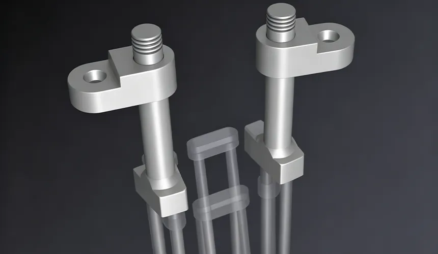
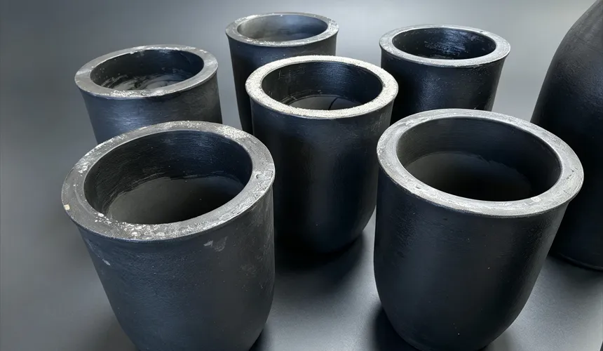
This project involves the customized development of a core graphite thermal field system for a single-crystal silicon growth furnace, tailored for a leading domestic photovoltaic enterprise. The system includes a complete set of components such as graphite crucibles, flow distributors, insulation sleeves, and electrodes, designed to support 12-inch large-scale single-crystal silicon wafer production lines. The primary objective is to enhance the efficiency of single-crystal silicon growth and improve product yield by optimizing the purity and structural design of graphite materials, thereby reducing photovoltaic module manufacturing costs and enabling high-efficiency mass production. The entire thermal field system must operate stably over long periods under temperatures exceeding 1500°C and in an inert gas-protected environment, meeting the stringent requirements of large-scale photovoltaic production.
2. Customer Requirements and Challenges
The core customer requirements include: first, the graphite material must meet photovoltaic-grade purity standards, with carbon impurity content below 5 ppm, to prevent contamination of silicon feedstock and ensure optimal photoelectric conversion efficiency in monocrystalline silicon wafers; second, the thermal field system must exhibit excellent high-temperature stability and uniform heat conduction, ensuring a stable temperature field during single-crystal silicon growth and minimizing crystal defects; third, component service life must support continuous production, reducing replacement frequency and downtime losses; fourth, components must be compatible with existing production line equipment dimensions, enabling quick installation and seamless integration.
Key challenges include: difficulty in controlling uniformity for large-sized graphite components, which can lead to localized density variations and thermal conductivity deviations; susceptibility of graphite to slight reactions with silicon vapor at high temperatures, affecting component longevity; and the need to balance material purity with production costs, avoiding excessive R&D that could drive up expenses beyond the customer's budget.
3. Production & Final Delivery
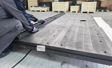
The production process uses high-purity graphite as the raw material, combined with petroleum coke and other auxiliary materials. Through isostatic pressing molding, component density uniformity is enhanced, followed by high-temperature graphitization to further purify the material and ensure carbon impurity levels meet specifications. For large-sized components, optimized mold design and sintering processes are employed, along with segmented temperature control during sintering to eliminate internal stresses and improve high-temperature stability. The inner walls of the flow guide tubes are polished to minimize silicon vapor adhesion and reduce reaction losses.
The complete graphite hot zone system is delivered, including on-site installation, commissioning, and trial operation, accompanied by a comprehensive user and maintenance manual and technical training to ensure smooth startup of the customer's production line. Prior to delivery, third-party testing confirms that all performance indicators meet customer requirements, with component service life 40% higher than the industry average.
4. Project Outcome
After implementation, the customer's single-crystal silicon growth efficiency increased by 15%, and the yield of single-crystal silicon wafers rose from 92% to 96%, significantly reducing production costs. The stable operation of the graphite thermal field system reduced production line downtime, lowering annual downtime losses by 30%. The successful application of this project has provided a reliable graphite solution for large-size single-crystal silicon wafer production in the photovoltaic industry, while also promoting technological upgrades and large-scale application of photovoltaic-grade graphite materials, helping enterprises enhance their market competitiveness.
 English